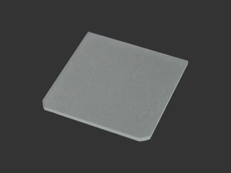
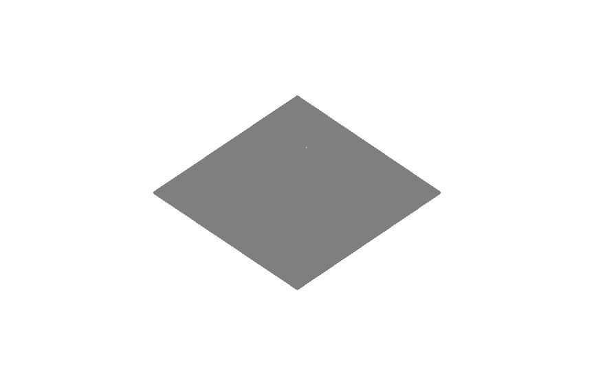
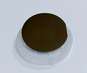
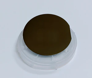
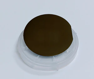
TGG Single Crystal Substrate: (111) 10 x 10 x. 0.5mm , 1 SP - TGGc1010S1
TGG singlecrystal Terbium Gallium Garne is an excellent magneto-optical crystal used in various Faraday device s(Rotator and Isolator) in the range of 400nm-1100nm, ( excluding 475 - 500nm.). which can replace YIG crystal
- Single crystal of TGG
- Size: 10 mm x 10 mm x 0.5mm
- Orientation: (111) +/-0.5 o
- Polish: One sides polished
- Surface roughness: 10A
|
Typical Properties
Main Advantage
Large Verdet Constant (35 Rad T-1m-1).
Low optical losses (<0.1%/cm)
High thermal conductivity (7.4W m-1K-1).
High laser damage threshold (>1GW/cm2).
Main ApplicationFaraday Rotator, Optical Isolator etc

|
Related Products
CdWO4 |
LSAT |
LaAlO3 |
MgO |
Film Coaters |
 |
 |
|
|
 |
| SrLaAlO4 | NdCaAlO4 |
SrTiO3 |
YSZ |
Wafer Boxes |
 |
 |
 |
|
 |
Product Information
Product Information
Shipping & Returns
Shipping & Returns

TGG Single Crystal Substrate: (111) 10 x 10 x. 0.5mm , 1 SP - TGGc1010S1
TGG Single Crystal Substrate: (111) 10 x 10 x. 0.5mm , 1 SP - TGGc1010S1
TGG singlecrystal Terbium Gallium Garne is an excellent magneto-optical crystal used in various Faraday device s(Rotator and Isolator) in the range of 400nm-1100nm, ( excluding 475 - 500nm.). which can replace YIG crystal
- Single crystal of TGG
- Size: 10 mm x 10 mm x 0.5mm
- Orientation: (111) +/-0.5 o
- Polish: One sides polished
- Surface roughness: 10A
|
Typical Properties
Main Advantage
Large Verdet Constant (35 Rad T-1m-1).
Low optical losses (<0.1%/cm)
High thermal conductivity (7.4W m-1K-1).
High laser damage threshold (>1GW/cm2).
Main ApplicationFaraday Rotator, Optical Isolator etc
|
Related Products
CdWO4 |
LSAT |
LaAlO3 |
MgO |
Film Coaters |
|
|
|
|
|
| SrLaAlO4 | NdCaAlO4 |
SrTiO3 |
YSZ |
Wafer Boxes |
|
|
|
|
|
$104.65
Original: $299.00
-65%TGG Single Crystal Substrate: (111) 10 x 10 x. 0.5mm , 1 SP - TGGc1010S1—
$299.00
$104.65Product Information
Product Information
Shipping & Returns
Shipping & Returns
Description
TGG singlecrystal Terbium Gallium Garne is an excellent magneto-optical crystal used in various Faraday device s(Rotator and Isolator) in the range of 400nm-1100nm, ( excluding 475 - 500nm.). which can replace YIG crystal
- Single crystal of TGG
- Size: 10 mm x 10 mm x 0.5mm
- Orientation: (111) +/-0.5 o
- Polish: One sides polished
- Surface roughness: 10A
|
Typical Properties
Main Advantage
Large Verdet Constant (35 Rad T-1m-1).
Low optical losses (<0.1%/cm)
High thermal conductivity (7.4W m-1K-1).
High laser damage threshold (>1GW/cm2).
Main ApplicationFaraday Rotator, Optical Isolator etc
|
Related Products
CdWO4 |
LSAT |
LaAlO3 |
MgO |
Film Coaters |
|
|
|
|
|
| SrLaAlO4 | NdCaAlO4 |
SrTiO3 |
YSZ |
Wafer Boxes |
|
|
|
|
|